- 您现在的位置:买卖IC网 > Sheet目录3896 > PIC16F505T-I/SL (Microchip Technology)IC MCU FLASH 1KX12 14SOIC
PIC12F508/509/16F505
DS41236E-page 32
2009 Microchip Technology Inc.
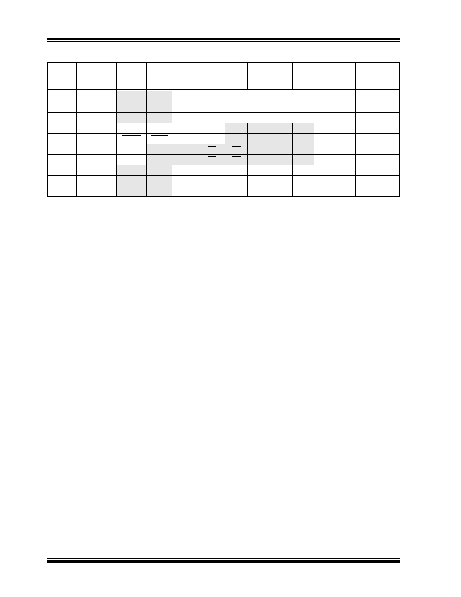
TABLE 5-1:
SUMMARY OF PORT REGISTERS
Address
Name
Bit 7
Bit 6
Bit 5
Bit 4
Bit 3
Bit 2
Bit 1
Bit 0
Value on
Power-On
Reset
Value on
All Other
Resets
N/A
TRISGPIO(1)
—
I/O Control Register
--11 1111
N/A
TRISB(2)
—
I/O Control Register
--11 1111
N/A
TRISC(2)
—
I/O Control Register
--11 1111
N/A
OPTION(1)
GPWU
GPPU
TOCS
TOSE
PSA
PS2
PS1
PS0
1111 1111
N/A
OPTION(2)
RBWU
RBPU
TOCS
TOSE
PSA
PS2
PS1
PS0
1111 1111
03h
STATUS(1)
GPWUF
—
PAO
TO
PD
Z
DC
C
0-01 1xxx
q00q quuu
(3)
03h
STATUS(2)
RBWUF
—
PAO
TO
PD
Z
DC
C
0-01 1xxx
q00q quuu(3)
06h
GPIO(1)
—
GP5
GP4
GP3
GP2
GP1
GP0
--xx xxxx
--uu uuuu
06h
PORTB(2)
—
RB5
RB4
RB3
RB2
RB1
RB0
--xx xxxx
--uu uuuu
07h
PORTC(2)
—
RC5
RC4
RC3
RC2
RC1
RC0
--xx xxxx
--uu uuuu
Legend:
Shaded cells are not used by Port registers, read as ‘0’. – = unimplemented, read as ‘0’, x = unknown, u = unchanged,
q
= depends on condition.
Note
1:
PIC12F508/509 only.
2:
PIC16F505 only.
3:
If Reset was due to wake-up on pin change, then bit 7 = 1. All other Resets will cause bit 7 = 0.
发布紧急采购,3分钟左右您将得到回复。
相关PDF资料
PIC12F509T-I/SN
IC MCU FLASH 1KX12 8SOIC
PIC10F200T-E/OT
IC PIC MCU FLASH 256X12 SOT23-6
006200516230000
CONN FFC/FPC 16POS 1MM R/A SMD
006200516230000+
CONN FFC/FPC 16POS 1MM R/A SMD
40FMN-BMT-A-TF
CONN FMN HSNG 40POS SNGL NOR SMD
0781191309
CONN FFC/FPC 30POS .5MM VERT SMD
046214012010800+
CONN FPC VERTICAL 0.5 MM 12POS
006200514230000+
CONN FFC/FPC 14POS 1MM R/A SMD
相关代理商/技术参数
PIC16F505T-I/SL040
制造商:Microchip Technology Inc 功能描述:MCCPIC16F505T-I/SL040 14 PIN 1.5 KB F
PIC16F505T-I/ST
功能描述:8位微控制器 -MCU 2 KB 72 RAM 12 I/O RoHS:否 制造商:Silicon Labs 核心:8051 处理器系列:C8051F39x 数据总线宽度:8 bit 最大时钟频率:50 MHz 程序存储器大小:16 KB 数据 RAM 大小:1 KB 片上 ADC:Yes 工作电源电压:1.8 V to 3.6 V 工作温度范围:- 40 C to + 105 C 封装 / 箱体:QFN-20 安装风格:SMD/SMT
PIC16F506-E/MG
功能描述:8位微控制器 -MCU 1.5KB 67 RAM 12 I/O RoHS:否 制造商:Silicon Labs 核心:8051 处理器系列:C8051F39x 数据总线宽度:8 bit 最大时钟频率:50 MHz 程序存储器大小:16 KB 数据 RAM 大小:1 KB 片上 ADC:Yes 工作电源电压:1.8 V to 3.6 V 工作温度范围:- 40 C to + 105 C 封装 / 箱体:QFN-20 安装风格:SMD/SMT
PIC16F506-E/P
功能描述:8位微控制器 -MCU 1.5KB FL 67 RAM 12I/O Comp Ext Temp RoHS:否 制造商:Silicon Labs 核心:8051 处理器系列:C8051F39x 数据总线宽度:8 bit 最大时钟频率:50 MHz 程序存储器大小:16 KB 数据 RAM 大小:1 KB 片上 ADC:Yes 工作电源电压:1.8 V to 3.6 V 工作温度范围:- 40 C to + 105 C 封装 / 箱体:QFN-20 安装风格:SMD/SMT
PIC16F506-E/SL
功能描述:8位微控制器 -MCU 1.5KB Flsh 67RM 12IO Comp 8B ADC Ext Temp RoHS:否 制造商:Silicon Labs 核心:8051 处理器系列:C8051F39x 数据总线宽度:8 bit 最大时钟频率:50 MHz 程序存储器大小:16 KB 数据 RAM 大小:1 KB 片上 ADC:Yes 工作电源电压:1.8 V to 3.6 V 工作温度范围:- 40 C to + 105 C 封装 / 箱体:QFN-20 安装风格:SMD/SMT
PIC16F506-E/ST
功能描述:8位微控制器 -MCU 1.5 KB Flash 67RAM12 I/O 8bit ADC RoHS:否 制造商:Silicon Labs 核心:8051 处理器系列:C8051F39x 数据总线宽度:8 bit 最大时钟频率:50 MHz 程序存储器大小:16 KB 数据 RAM 大小:1 KB 片上 ADC:Yes 工作电源电压:1.8 V to 3.6 V 工作温度范围:- 40 C to + 105 C 封装 / 箱体:QFN-20 安装风格:SMD/SMT
PIC16F506-I/MG
功能描述:8位微控制器 -MCU 1.5 KB Flash 73 RAM 12 I/O RoHS:否 制造商:Silicon Labs 核心:8051 处理器系列:C8051F39x 数据总线宽度:8 bit 最大时钟频率:50 MHz 程序存储器大小:16 KB 数据 RAM 大小:1 KB 片上 ADC:Yes 工作电源电压:1.8 V to 3.6 V 工作温度范围:- 40 C to + 105 C 封装 / 箱体:QFN-20 安装风格:SMD/SMT
PIC16F506-I/P
功能描述:8位微控制器 -MCU 1.5KB 72 RAM 12 I/O Ind Temp PDIP14 RoHS:否 制造商:Silicon Labs 核心:8051 处理器系列:C8051F39x 数据总线宽度:8 bit 最大时钟频率:50 MHz 程序存储器大小:16 KB 数据 RAM 大小:1 KB 片上 ADC:Yes 工作电源电压:1.8 V to 3.6 V 工作温度范围:- 40 C to + 105 C 封装 / 箱体:QFN-20 安装风格:SMD/SMT